Molecular-Level Insight into Semiconductor Nanocrystal Surfaces
Abstract
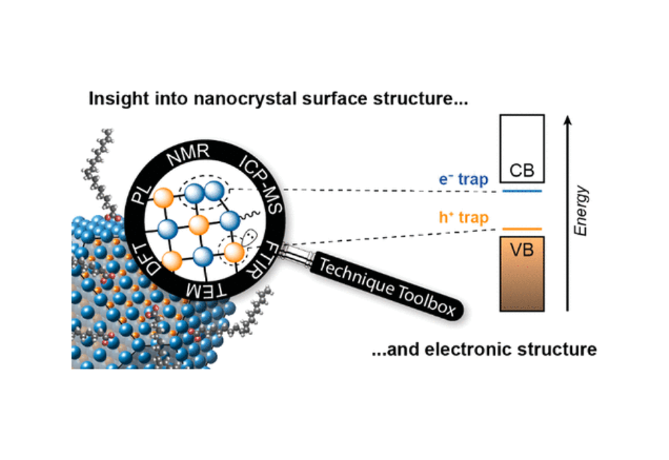
Semiconductor nanocrystals exhibit attractive photophysical properties for use in a variety of applications. Advancing the efficiency of nanocrystal-based devices requires a deep understanding of the physical defects and electronic states that trap charge carriers. Many of these states reside at the nanocrystal surface, which acts as an interface between the semiconductor lattice and the molecular capping ligands. While a detailed structural and electronic understanding of the surface is required to optimize nanocrystal properties, these materials are at a technical disadvantage: unlike molecular structures, semiconductor nanocrystals lack a specific chemical formula and generally must be characterized as heterogeneous ensembles. Therefore, in order for the field to improve current nanocrystal-based technologies, a creative approach to gaining a “molecular-level” picture of nanocrystal surfaces is required. To this end, an expansive toolbox of experimental and computational techniques has emerged in recent years. In this Perspective, we critically evaluate the insight into surface structure and reactivity that can be gained from each of these techniques and demonstrate how their strategic combination is already advancing our molecular-level understanding of nanocrystal surface chemistry.
Citation
Molecular-Level Insight into Semiconductor Nanocrystal Surfaces
Carolyn L. Hartley, Melody L. Kessler, and Jillian L. Dempsey
Journal of the American Chemical Society 2021 143 (3), 1251-1266
DOI: 10.1021/jacs.0c10658