Characterizing Density and Spatial Distribution of Trap States in Ta3N5 Thin Films for Rational Defect Passivation
Abstract
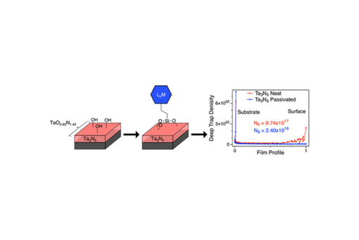
Tantalum nitride (Ta3N5) has gained significant attention as a potential photoanode material, yet it has been challenged by material quality issues. Defect-induced trap states are detrimental to the performance of any semiconductor material. Beyond influencing the performance of Ta3N5 films, defects can also accelerate the degradation in water during desired electrochemical applications. Defect passivation has provided an enormous boost to the development of many semiconductor materials but is currently in its infancy for Ta3N5. This is in part due to a lack of experimental understanding regarding the spatial and energetic distribution of trap states throughout Ta3N5 thin films. Here, we employ drive-level capacitance profiling (DLCP) to experimentally resolve the spatial and energetic distribution of trap states throughout Ta3N5 thin films. The density of deeper energetic traps is found to reach ∼2.5 to 6 × 1022 cm–3 at the interfaces of neat Ta3N5 thin films, over an order of magnitude greater than the bulk. In addition to the spatial profile of deep trap states, we report neat Ta3N5 thin films to be highly n-type in nature, owning a free carrier density of ∼9.74 × 1017 cm–3. This information, coupled with the present understanding of native oxide layers on Ta3N5, has facilitated the rational design of a targeted passivation strategy that simultaneously provides a means for catalyst immobilization. Loading catalyst via silatrane moieties suppresses the density of defects at the surface of Ta3N5 thin films by two orders of magnitude, while also reducing the free carrier density of films by over one order of magnitude, effectively dedoping the films to ∼2.40 × 1016 cm–3. The surface passivation of Ta3N5 films translates to suppressed defect-induced trapping and recombination of photoexcited carriers, as determined through absorption, photoluminescence, and transient photovoltage. This illustrates how developing a deeper understanding of the distribution and influence of defects in Ta3N5 thin films has the potential to guide future works and ultimately accelerate the integration and development of high-performance Ta3N5 thin film devices.
Citation
Characterizing Density and Spatial Distribution of Trap States in Ta3N5 Thin Films for Rational Defect Passivation
Peter N. Rudd, Stephen J. Tereniak, and Rene Lopez
ACS Applied Materials & Interfaces 2023 15 (6), 7969-7977
DOI: 10.1021/acsami.2c19275